Latest News & Events
Voltage Blooming: an open letter and report to the industry

“Voltage Blooming” of Real-Time X-ray Images: Ensuring accuracy when measuring the percentage of voids in BGA solder bonds
By Gilbert Zweig, President, Glenbrook Technologies, Inc.
Ever since the introduction of plastic ball grid array (PBGA) packages, concerns have been raised about the possible effects of solder voids on board-level reliability. A study was conducted to determine the effect of PBGA solder voids on the physical reliability of the bond.
In the experiment, a series of test assemblies was prepared, reflowed and put through accelerated thermal cycling. The result of the experiment led to a number of interesting observations. First, assemblies having very little voiding failed “significantly earlier” than assemblies with some voiding, indicating that a certain degree of voiding actually contributed to board reliability.
Second, in assemblies with cracks in the solder, the voids did not change the path of propagating cracks. However, since assemblies with voids demonstrated a higher degree of reliability, it may be that voids “have some crack arresting properties.”
Finally, through the use of real-time X-ray inspection and image analysis software, the study concluded that, for assemblies in which solder joint voids constituted up to 24 percent of the total pad area, the voids had no negative effect on board reliability. “In fact, PBGA solder joints with voids had 16 percent better reliability than those without voids.”
This study casts a whole new light on the role of BGA solder voids and on the critical importance of measuring void sizes accurately. Many electronics manufacturers have come to rely on the measurement of solder voids as a pass/fail criterion when inspecting assemblies containing one or more BGA-type components. All boards containing voids larger than a certain size are rejected and returned to rework. This practice is valid when the measurement of the voids is precise and reliable.
However, the possibility exists that perfectly good BGA assemblies may be rejected due to inaccurate solder void measurement. This could have disastrous economic consequences for many manufacturers, if the result is that their reject and rework rates are inflated unnecessarily.
The most common method of inspecting the solder bonds of BGA packages is to use real-time X-ray inspection systems. The creation of a real-time X-ray image requires an X-ray source to provide and direct the X-ray flux through the BGA assembly. An X-ray camera uses an X-ray-luminescent phosphor to convert the X-ray image into a visible light image. The X-ray image impinges on the X-ray camera, where an X-ray luminescent phosphor converts the pattern of varying X-ray intensity into a pattern of varying light intensity. The light image is usually amplified and converted to a video image.
A limited number of commercially available X-ray camera configurations are used by many companies to construct conventional BGA real-time X-ray inspection systems. The most popular of these is the medical-type image intensifier, which employs the X-ray phosphor Cesium Iodide in the photocathode. A second popular X-ray camera configuration is one in which an X-ray phosphor is coated onto the glass window of a vidicon video tube.
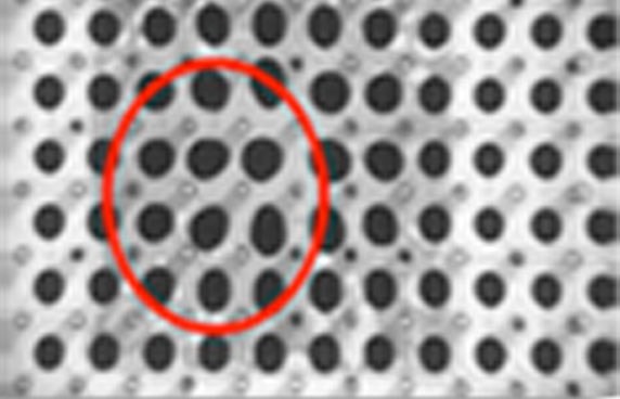
One troubling characteristic of both of these types of X-ray cameras is a phenomenon which can be described as Voltage Blooming. The way Voltage Blooming manifests itself is that, as the voltage of the X-ray tube control is increased, the white areas of the X-ray image, which represent solder voids, encroach on the black areas, causing the white portions of the image to appear to grow larger as the black areas diminish. Thus, the same void that occupies less than ten percent of a BGA solder bond at 57 kV may appear to consume up to 50 percent of the bond at 76 kV (Figure 1). This effect appears to be related to the choice and design of the X-ray luminescent phosphor used in the X-ray camera.
 |
 |
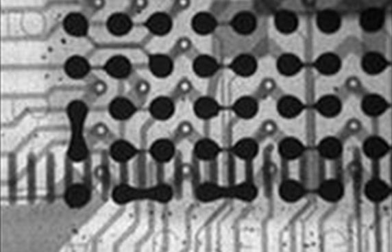
| FIGURE 1: BGA solder bonds, imaged at 57 kV and 76 kV with conventional X-ray camera technology, demonstrate the Voltage Blooming effect: at higher voltage, solder voids appear larger in relation to the bond area. | FIGURE 2: Glenbrook’s patented X-ray camera technology eliminates the Voltage Blooming effect: when imaged at 50 kV and 70 kV, the size of the solder voids remains constant in relation to the bond area. |
Consider the consequence of the Voltage Blooming effect on the critical requirement of determining the maximum percentage of void levels required for a BGA assembly to pass inspection. It is evident that conventional X-ray camera configurations make it impossible to obtain an accurate measurement of solder void area, because the solder void size is determined by the particular voltage to which the X-ray tube is set. Further, that size can appear to increase or decrease in relation to the total bond area when the voltage level is increased or decreased.
In order to obtain accurate and reliable measurements of solder void sizes in relation to total solder bond area, a different type of X-ray camera is required. The X-ray camera technology developed and patented by Glenbrook Technologies, and employed in all the company’s real-time X-ray inspection systems, achieves the degree of measurement consistency required to determine solder void size for varying voltage levels. (Figure 2)
As initially developed, this camera is unique in its ability to provide X-ray images of relatively high resolution (15-20 lp/mm at 1:1 geometric magnification) at relatively low X-ray anode power (less than 1 watt) across a broad range of X-ray energies, with X-ray tube parameters of 35 kV and 25 microamps. Among commercially available cameras, it is also one of the most sensitive, capable of producing X-ray images at voltages as low at 15kV.
In comparison, the resolution of the typical fluoroscopic image intensifier used in conventional industrial and medical imaging systems at the same geometric magnification is approximately 3 lp/mm. Further, in order to produce this low-resolution image, these systems require X-ray anode power levels of 60 watts or more, operating at 70 to 120 kV.
The Glenbrook camera design is based on the company’s experience in X-ray phosphor technology, dating back to 1970. Additionally, an ongoing program of research into X-ray technology has led to significant product enhancements over the years. Most recently, a new phosphor design has resulted in a thirty percent improvement in resolution, while maintaining the distortion-free qualities that support precise BGA solder void measurement.
Real-time X-ray inspection systems that incorporate this camera have achieved widespread use by both printed circuit board fabricators and electronics assemblers worldwide over the past two decades. In addition to the camera’s consistency in representing solder void sizes, its benefits include lower initial system cost, lower operating cost and improved performance for particular applications.
The combination of low power and high sensitivity permits X-ray inspection of both low density and high density BGA packages. Additionally, the X-ray system may be housed in relatively small and lightweight systems ranging from compact, portable units to console models, plus a fully enclosed workstation model, to meet a variety of production requirements.
The low power level also extends the life of the X-ray tube dramatically, reducing operating costs. In addition, evidence indicates that some types of electronic components may be damaged by high levels of ionizing radiation, but not by a low power system. Finally, low voltage X-ray imaging allows the visualization of details such as aluminum wires in integrated circuits, which cannot be achieved at higher X-ray voltages.
The full range of benefits provided by Glenbrook’s X-ray camera technology is available in the modular, upgradeable RTX Series of real-time X-ray systems designed for rapid inspection of multi-layer and assembled printed circuit boards. These include the portable RTX-Mini™, which may be used on a desk or countertop, or hand-carried into a production environment.
The console model RTX-113, designed for reliable operation in a production environment, also supports easy customizing for specialized applications such as small hole drilling, BGA inspection, large backplanes and components.
The Jewel Box, provides high resolution and high magnification for laboratory applications and failure analysis of microBGAs, flip chips, ICs and other advanced components.
A wide range of options extends the capabilities of these real-time X-ray inspection systems. These include software to measure and characterize solder bond voids, a zoom camera for 7X to 40X magnification, a 10-micron X-ray source with variable magnification up to 500X, plus a variety of image enhancement, measurement, printing and downloading capabilities.
From this variety of systems and options, all built around patented real-time X-ray camera technology, manufacturers may select an inspection system customized to specific production requirements and upgradeable to meet future needs, while maintaining the accuracy required to obtain precise measurement of BGA solder voids.
References
“The Effects of Solder Joint Voiding on Plastic Ball Grid Array Reliability,”
Donald R. Banks, et. al.,
1996 SMI Proceedings, p. 121-126. All subsequent quotes in this article are excerpted from the cited paper.